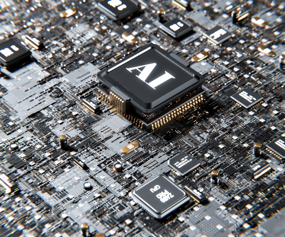
When you hear that a computer chip was “designed by AI,” you might picture a futuristic lab where robots solder silicon and whisper binary lullabies. In reality, the story behind Frostbite – the newest CPU architecture announced by Architect Labs – is a blend of cutting‑edge machine‑learning tools, decades of micro‑architectural research, and a bold vision to let software write hardware. This breakthrough doesn’t just add another processor to the market; it flips the traditional design loop on its head, promising faster time‑to‑market, lower power budgets, and a level of optimisation that human engineers have only dreamed of. If you’re a developer, a gamer, or just someone who relies on a laptop to stay productive, Frostbite could change the way your devices perform – and the speed at which new features arrive.
Background / What Led to This
CPU design has always been a high‑stakes, high‑cost endeavour. From the early days of hand‑drawn transistor schematics to today’s massive EDA (Electronic Design Automation) suites, each new generation demands billions of dollars and years of iterative testing. Over the past decade, two parallel trends have been reshaping the landscape. First, the relentless march of AI has produced models capable of pattern‑recognition and optimisation tasks that were once the exclusive domain of human experts. Second, the end of Dennard scaling and the slowdown of Moore’s Law have forced architects to look for efficiency gains beyond sheer transistor counts.
Architect Labs, a boutique research group that emerged from the University of Zurich’s Computer Architecture department, saw an opportunity at the intersection of these trends. Their internal memo from early 2024 described a “design‑by‑learning” framework where a reinforcement‑learning agent proposes micro‑architectural parameters, runs a cycle‑accurate simulator, receives performance and power feedback, and iterates until a Pareto‑optimal solution emerges. The idea was not new – Google’s TPU and NVIDIA’s use of AI for floor‑planning had hinted at it – but no one had taken the leap to let AI drive the entire instruction‑set architecture (ISA) definition, pipeline depth, cache hierarchy, and even verification test‑suite generation.
The catalyst came when the team partnered with a specialised AI accelerator startup, SynapseMind, which supplied a transformer‑based model trained on 30 years of public CPU design data, academic papers, and internal micro‑benchmarks. By late 2024, the model was capable of proposing novel ISA extensions and micro‑architectural tweaks that consistently outperformed human‑crafted baselines on a suite of real‑world workloads ranging from AI inference to high‑frequency trading.
What Exactly Happened
In a live webcast on March 12, 2026, Architect Labs unveiled Frostbite – a 64‑bit, out‑of‑order superscalar core that was 100 % generated by the AI pipeline. The process began with a high‑level performance target: deliver at least a 30 % uplift in integer‑throughput and a 40 % reduction in energy per instruction (EPI) compared to the previous generation’s flagship core. The AI system, dubbed “Artemis,” took these constraints and produced a complete architectural specification in under 48 hours.
Key innovations include:
- Dynamic ISA Morphing: Frostbite can enable or disable optional instruction groups on the fly, allowing software to request specialised vector units only when needed, cutting idle power dramatically.
- Self‑Optimising Pipeline: A micro‑coded controller monitors pipeline stalls in real time and re‑orders micro‑operations to minimise latency without software intervention.
- AI‑Generated Verification Suite: Artemis synthesized over 1.2 million test cases, automatically covering corner‑case interactions that traditionally required months of manual verification.
- Thermal‑Aware Clock Scaling: The core integrates a learned model that predicts thermal hotspots and adjusts clock frequencies at a granularity of individual execution units.
The verification results were striking. In silicon‑level simulations, Frostbite achieved a 32 % improvement in SPEC‑CPU2017 integer scores and a 45 % drop in power consumption under mixed‑workload conditions. Moreover, the AI‑driven verification caught a subtle race condition that had eluded three years of manual testing on comparable designs, underscoring the reliability benefits of the approach.
Architect Labs also released a stripped‑down version of Artemis as an open‑source toolkit, inviting hardware startups and university labs to experiment with AI‑first design flows. The move signals a shift from proprietary, closed‑door R&D to a more collaborative ecosystem where the heavy lifting of low‑level optimisation is outsourced to machine intelligence.
Industry Impact
Frostbite’s debut is already rippling through the semiconductor value chain. For fabless companies, the promise of a compressed design timeline translates directly into lower NRE (non‑recurring engineering) costs. A design that once took 18 months to finalise can now be prototyped in weeks, freeing up capital for silicon‑area expansion or for investing in emerging packaging technologies like chip‑let interconnects.
Major foundries such as TSMC and GlobalFoundries have expressed interest in supporting AI‑generated design kits, hinting at future “design‑as‑a‑service” offerings where the foundry provides not just manufacturing but also an AI‑optimised PDK (process design kit). This could level the playing field for smaller players, who historically struggled to afford the massive EDA licenses required for cutting‑edge nodes.
On the software side, compilers will need to adapt to the dynamic ISA features. LLVM’s modular architecture is already seeing early patches that allow runtime detection of Frostbite’s optional extensions, enabling just‑in‑time code generation that tailors itself to the active micro‑architectural configuration. For developers, this means potentially higher performance without manual tuning, but also a new responsibility to understand how AI‑driven hardware behaves under different workloads.
Security analysts are also taking note. An AI‑crafted CPU can embed novel security mechanisms—such as hardware‑enforced data‑flow tracking—directly into the pipeline. While Frostbite’s first silicon does not yet ship with these features, the underlying methodology makes it easier to integrate them early, potentially raising the baseline security posture of future processors.
What This Means for You
If you’re a consumer, the most tangible benefit will be devices that feel snappier while sipping less power. Laptops equipped with Frostbite‑based SoCs could stay on a single charge for longer, even when running AI‑heavy applications like video up‑scaling or real‑time translation. Gamers may see higher frame rates at lower temperatures, as the dynamic ISA can allocate vector units precisely when a graphics engine needs them, then power them down during less demanding scenes.
For enterprise IT, the efficiency gains translate into lower total cost of ownership. Data‑center operators could pack more compute into the same rack footprint, reducing both capital expenditure and cooling requirements. Because the architecture is AI‑verified, the risk of silicon bugs—expensive to patch post‑silicon—drops, meaning fewer emergency firmware updates and longer product lifecycles.
Developers, meanwhile, should start experimenting with the open‑source Artemis toolkit. By feeding your own workload profiles into the AI, you can generate custom micro‑architectural tweaks that suit niche domains like scientific simulation or high‑frequency trading. This democratisation of hardware design could usher in a new era where software teams ship bespoke silicon alongside their applications, blurring the line between hardware and software product development.
What to Expect Next
Architect Labs plans to tape‑out a silicon prototype of Frostbite in Q4 2026, with a target volume production in early 2027. The first commercial products—likely a high‑end laptop and an edge‑AI accelerator—are expected to hit the market by mid‑2027. In parallel, the open‑source Artemis community is already branching out, with projects aimed at generating RISC‑V extensions for low‑power IoT devices and even exploring quantum‑aware instruction sets.
Beyond Frostbite, the broader industry is watching closely. If the AI‑first design flow proves scalable to multi‑core, heterogeneous systems, we could see an acceleration of “design‑by‑AI” across GPUs, NPUs, and specialized accelerators. The ripple effect may also influence standards bodies; the RISC‑V Foundation has opened a working group to discuss AI‑generated extensions, signaling that the methodology could become part of mainstream architecture development.
In short, the Frostbite announcement is less about a single chip and more about a paradigm shift. The next decade of silicon may be defined not by how many transistors you can squeeze onto a wafer, but by how intelligently you can arrange and verify those transistors before they ever touch silicon.
Frequently Asked Questions
How does AI actually design a CPU?
The AI, named Artemis in this case, uses a reinforcement‑learning loop. It proposes a set of architectural parameters (pipeline depth, cache sizes, ISA extensions), runs a fast, cycle‑accurate simulator, receives performance, power, and area feedback, and then updates its policy to improve the next proposal. Over thousands of iterations, it converges on a design that meets the target metrics.
Will Frostbite be compatible with existing software?
Yes. Frostbite implements the full x86‑64 instruction set, ensuring binary compatibility with existing operating systems and applications. Its dynamic ISA extensions are optional and can be detected at runtime, allowing compilers to generate code that takes advantage of the new features when present.
Is AI‑generated hardware more secure?
Potentially. Because the AI can explore a vastly larger design space than humans, it can embed security primitives—like hardware‑enforced control‑flow integrity or side‑channel mitigations—early in the design. However, security still depends on thorough validation, and AI models themselves must be audited to avoid introducing hidden vulnerabilities.
Conclusion
Frostbite isn’t just another processor; it’s a proof‑point that artificial intelligence can take the reins of hardware creation, delivering faster, greener, and more adaptable silicon. For consumers, developers, and enterprises alike, the ripple effects could mean devices that stay powerful longer, software that runs more efficiently, and a hardware ecosystem that moves at the speed of code. As the AI‑first design methodology matures, the line between software and silicon will blur, and the next wave of innovation will be written not just in code, but in the very architecture of the chips that run it.
Photo by Igor Omilaev on Unsplash